
STM32: using the LTDC display controller

The STM32 LTDC has a peripheral called LTDC LCD TFT Display Controller which provides a digital parallel interface (DPI) for a variety of LCD and TFT panels. It sends RGB data in parallel to the display and generates signals for horizontal and vertical synchronization (HSYNC, VSYNC), as well as pixel clock (PCLK) and not data enable (DE) signals:
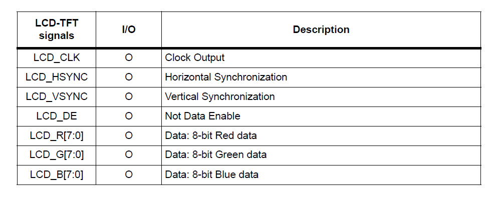
figure 1: LTDC RGB interface signals
RGB interface synchronization signals
LTDC synchronous timing parameters are configurable: a synchronous timing generator block inside the LTDC generates the horizontal and vertical synchronization signals, the pixel clock and not data enable signals. The configurable timing parameters are:
- LTDC_SSCR Synchronization Size Configuration Register, configured by programming the values HSYNC width – 1 and VSYNC width – 1
- LTDC_BPCR Back Porch Configuration Register, configured by programming the accumulated values HSYNC width + horizontal back porch – 1 and VSYNC width + vertical back porch – 1
- LTDC_AWCR Active Width Configuration Register, configured by programming the accumulated values HSYNC width + horizontal back porch + active width – 1 and VSYNC width + vertical back porch + active height – 1
- LTDC_TWCR Total Width Configuration Register, configured by programming the accumulated values HSYNC width + horizontal back porch + active width + horizontal front porch – 1 and VSYNC width + vertical back porch + active height + vertical front porch – 1
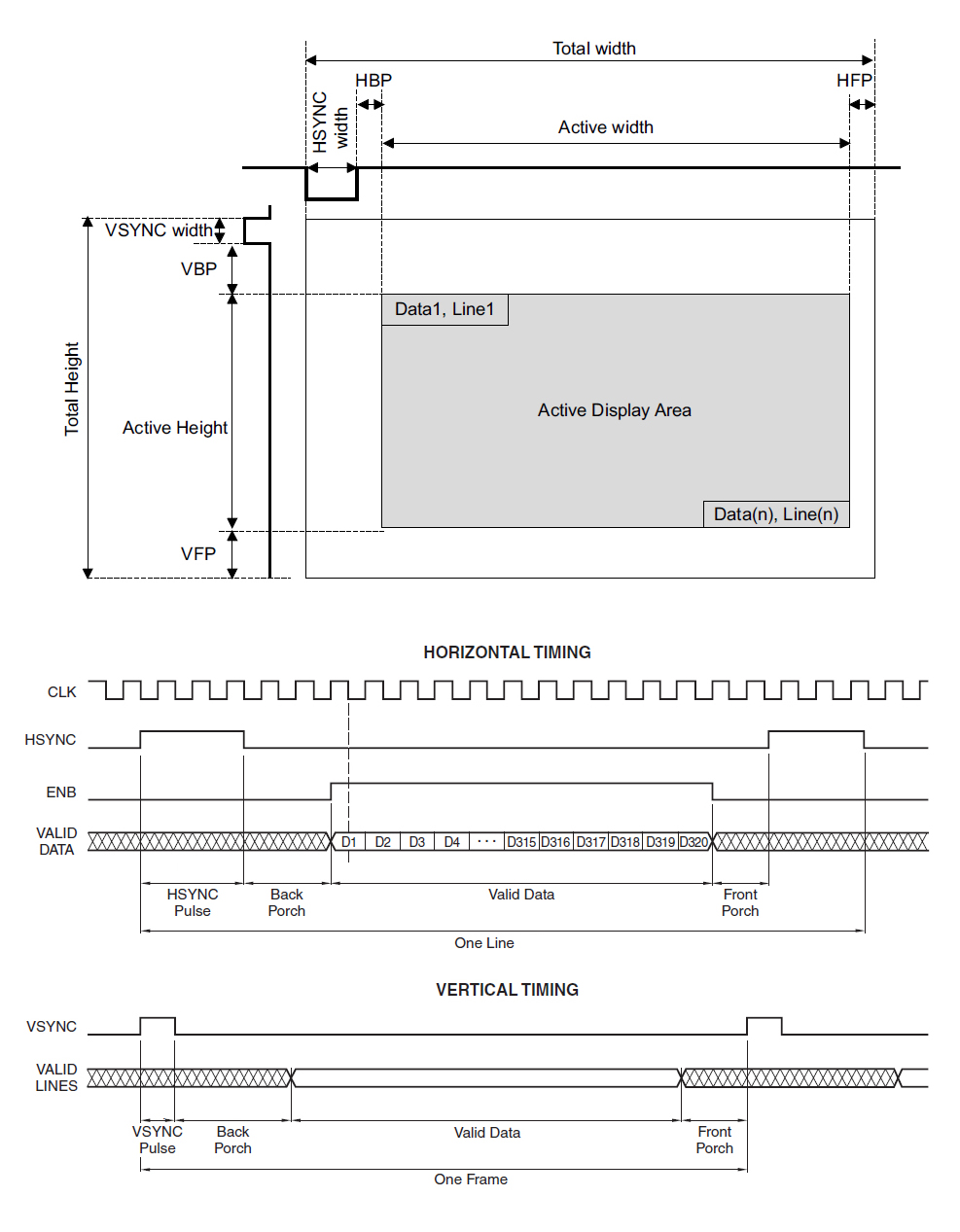
figure 2: RGB interface timing and horizontal/vertical synchronization, pixel clock and data enable signals
Horizontal timing signal widths are in units of pixel clocks, while vertical timing signal widths are in units of horizontal scan lines. The HSYNC, VSYNC, pixel clock and not data enable signal polarities can be configured to active high or active low in the LTDC_GCR Global Control Register (not data enable signal must be configured inverted with respect to the data enable signal in the display datasheet). The datasheet of the panel generally provides the timing parameters for the display:
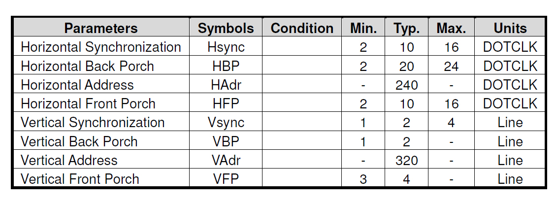
figure 3: RGB panel timing signals
Configuring the timing signals is the first thing to do to initialize the LTDC controller. The function HAL_LTDC_MspInit() initializes the low level details of the LTDC peripheral (clock and GPIOs):
/* initialize LTDC */ HAL_LTDC_MspInit(<dc); // initialize LTDC clock and pins LTDC->GCR &= ~(LTDC_GCR_HSPOL | LTDC_GCR_VSPOL | LTDC_GCR_DEPOL | LTDC_GCR_PCPOL); // synchronization signal polarities LTDC->SSCR = 9 << LTDC_SSCR_HSW_Pos | 1 << LTDC_SSCR_VSH_Pos; // HSYNC and VSYNC length LTDC->BPCR = 29 << LTDC_BPCR_AHBP_Pos | 3 << LTDC_BPCR_AVBP_Pos; // horizontal and vertical accumulated back porch LTDC->AWCR = 269 << LTDC_AWCR_AAW_Pos | 323 << LTDC_AWCR_AAH_Pos; // accumulated active width and height LTDC->TWCR = 279 << LTDC_TWCR_TOTALW_Pos | 327 << LTDC_TWCR_TOTALH_Pos; // accumulated total width and height
A constant background color can be configured in LTDC_BCCR Background Color Configuration Register (eight bits per channel are used in this register to select a solid RGB color):
LTDC->BCCR = 0x00 << LTDC_BCCR_BCRED_Pos | 0xFF << LTDC_BCCR_BCGREEN_Pos | 0x00 << LTDC_BCCR_BCBLUE_Pos; // background color (green)
The background color is used for blending with the bottom layer.
Layer configuration
The LTDC has two layers which can be configured, enabled and disabled independently, each with its own FIFO buffer. Layer order is fixed and layer2 is alway on top of layer1. Layer can be enabled writing the LEN Layer Enable bit in the LTDC_LxCR Layer x Control Register. Each layer gets its data from a framebuffer in memory and the start address is written in LTDC_LxCFBAR Layer x Color Frame Buffer Address Register. The frame buffer contains the display frame data in one of eight configurable pixel format: LTDC_LxPFCR Layer x Pixel Format Configuration Register is configured to choose the pixel format used to store data into the frame buffer. The available pixel formats are:
- ARGB8888
- RGB888
- RGB565
- ARGB1555
- ARGB4444
- L8 (8 bit luminance)
- AL44 (4 bit alpha, 4 bit luminance)
- AL88 (8 bit alpha, 8 bit luminance)
The pixel data are read from the frame buffer and converted to the LTDC internal 32-bit pixel format ARGB8888:
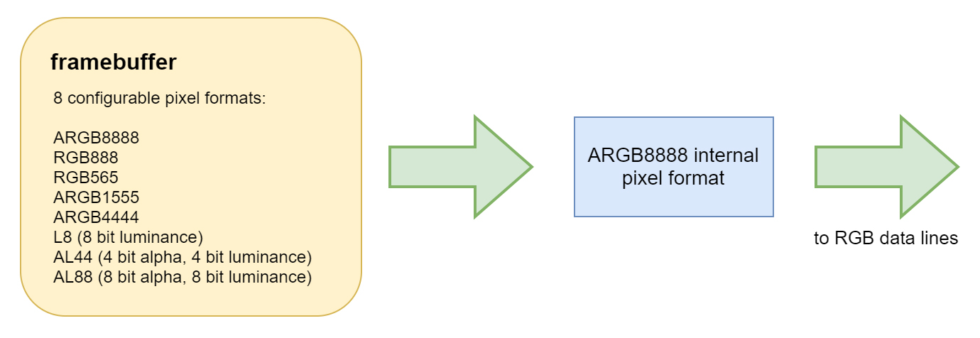
figure 4: whatever the framebuffer pixel format the LTDC converts the data into the internal 32 bit ARGB8888 pixel format
Each layer can be positioned and resized inside the active area indicating the start and stop position of the visible window in the LTDC_LxWHPCR Layer x Window Horizontal Position Configuration Register and LTDC_LxWVPCR Layer x Window Vertical Position Configuration Register. These parameters select the first and last visible pixels of a line and the first and last visible lines in the window. The values must includes the timing signals (HSYNC and VSYNC) width and the back porch width programmed into LTDC_BPCR register. In this case the accumulated horizontal back porch is 30 – 1, so the active area starts at 30 and the image is 240 pixel wide so horizontal window stop position is 30 + 240 – 1 = 269 (same for the vertical start and stop positions):
/* configure layer 1 */
LTDC_Layer1->WHPCR = 269 << LTDC_LxWHPCR_WHSPPOS_Pos | 30 << LTDC_LxWHPCR_WHSTPOS_Pos;          // window horizontal start/stop positions
LTDC_Layer1->WVPCR = 323 << LTDC_LxWVPCR_WVSPPOS_Pos | 4 << LTDC_LxWVPCR_WVSTPOS_Pos;           // window vertical start/stop positions
LTDC_Layer1->PFCR = 0x01;                                                                       // RGB888 pixel format
LTDC_Layer1->CFBAR = (uint32_t)framebuffer;                                                     // frame buffer start address
The frame buffer has a configurable line length (in bytes) in the LTDC_LxCFBLR Layer x Color Frame Buffer Length Register and a configurable total number of lines in the LTDC_LxCFBLNR Layer x Color Frame Buffer Line Number Register. It also has a configurable line pitch, which indicates the distance in bytes between the start of a line and the beginning of the next line, also configured in the LTDC_LxCFBLR register, and expressed in bytes. These parameters are used by the LTDC to fetch data from the frame buffer to the layer FIFO. If set to less byte than needed, a FIFO underrun interrupt will trigger (if enabled), if set to more bytes than required the rest of the data loaded into the layer’s FIFO is discarded.
LTDC_Layer1->CFBLR = 240 * 3 << LTDC_LxCFBLR_CFBP_Pos | 240 * 3 + 3 << LTDC_LxCFBLR_CFBLL_Pos;  // frame buffer line length and pitch
LTDC_Layer1->CFBLNR = 320;                                                                      // frame buffer line number
Line length parameter is the number of bytes in a line plus three (so the total line length is number of pixels * bits per pixel + 3). These parameters, together with the layer windowing settings, are useful if we want to display part of an image contained in the frame buffer, as I’ll show later.
Each layer can also have a default color, configured into the LTDC_LxDCCR Layer x Default Color Configuration Register, in ARGB8888 format, that is used outside the layer window or when a layer is disabled:
LTDC_Layer1->DCCR = 0xFF << LTDC_LxDCCR_DCALPHA_Pos | 0xFF << LTDC_LxDCCR_DCGREEN_Pos; // layer default color (solid green)
A constant alpha blending value is configured into the LTDC_LxCACR Layer x Constant Alpha Configuration Register, and controls the alpha blending with the underlying layers. In this case the value 255 (which is divided by 255 by hardware to get a value between 0 and 1) indicates a solid color:
LTDC_Layer1->CACR = 255; // constant alpha
Blending order is fixed and if both layers are enabled, first layer 1 is blended with the background and then layer 2 is blended with the result:
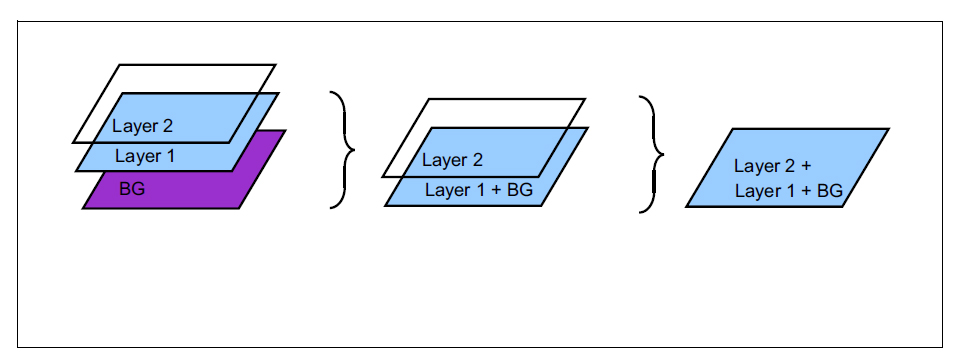
figure 5: layer blending
Then the layer is enabled by writing the LEN bit into the LTDC_LxCR LTDC Layer x Control Register:
LTDC_Layer1->CR |= LTDC_LxCR_LEN; // enable layer1
Shadow configuration registers
Some configuration registers are shadowed, meaning their programmed values are stored into shadow registers (not accessible to the programmer) and reloaded into the actual configuration registers based on the configuration of the LTDC_SRCR Shadow Reload Configuration Register: if this register is written with the IMR Immediate Reload bit the registers are reloaded immediately (as soon as the IMR bit is set the registers are reloaded), if the Vertical Blanking Reload bit is written the registers are reloaded with the new values during the vertical blanking period (at the beginning of the first line after the active display area). These bits are set in software and cleared by hardware when shadow registers are reloaded:
/* reload shadow registers and enable LTDC */
LTDC->SRCR = LTDC_SRCR_IMR;     // immediate shadow registers reload (before enabling LTDC)
LTDC->GCR |= LTDC_GCR_LTDCEN;   // enable LTDC
The registers read the old values until they’re reloaded and if a new value is written before they’re reloaded the previous value is overwritten. Most of the layers’ configuration registers are shadowed so they must be reloaded after being configured and before anabling the LTDC. The complete LTDC_init() function looks like this:
void LTDC_init(void)
{
/* initialize LTDC */
HAL_LTDC_MspInit(<dc); // initialize LTDC low level hardware (clock and pins)
/* configure LTDC general parameters */
LTDC->GCR &= ~(LTDC_GCR_HSPOL | LTDC_GCR_VSPOL | LTDC_GCR_DEPOL | LTDC_GCR_PCPOL); // signal polarities
LTDC->SSCR = 9 << LTDC_SSCR_HSW_Pos | 1 << LTDC_SSCR_VSH_Pos; // HSYNC and VSYNC length
LTDC->BPCR = 29 << LTDC_BPCR_AHBP_Pos | 3 << LTDC_BPCR_AVBP_Pos; // horizontal and vertical accumulated back porch
LTDC->AWCR = 269 << LTDC_AWCR_AAW_Pos | 323 << LTDC_AWCR_AAH_Pos; // accumulated active width and height
LTDC->TWCR = 279 << LTDC_TWCR_TOTALW_Pos | 327 << LTDC_TWCR_TOTALH_Pos; // accumulated total width and height
LTDC->BCCR = 0xFF << LTDC_BCCR_BCGREEN_Pos; // green background color
/* configure layer 1 */
LTDC_Layer1->WHPCR = 269 << LTDC_LxWHPCR_WHSPPOS_Pos | 30 << LTDC_LxWHPCR_WHSTPOS_Pos; // window horizontal start/stop positions
LTDC_Layer1->WVPCR = 323 << LTDC_LxWVPCR_WVSPPOS_Pos | 4 << LTDC_LxWVPCR_WVSTPOS_Pos; // window vertical start/stop positions
LTDC_Layer1->PFCR = 0x01; // RGB888 pixel format
LTDC_Layer1->DCCR = 0xFF << LTDC_LxDCCR_DCALPHA_Pos | 0xFF << LTDC_LxDCCR_DCGREEN_Pos; // layer default color
LTDC_Layer1->CFBAR = (uint32_t)image; // frame buffer start address
LTDC_Layer1->CFBLR = 240 * 3 << LTDC_LxCFBLR_CFBP_Pos | 240 * 3 + 3 << LTDC_LxCFBLR_CFBLL_Pos; // frame buffer line length and pitch
LTDC_Layer1->CFBLNR = 320; // frame buffer line number
LTDC_Layer1->CACR = 255; // constant alpha
LTDC_Layer1->CR |= LTDC_LxCR_LEN; // enable layer1
LTDC->SRCR = LTDC_SRCR_IMR; // immediate shadow registers reload
LTDC->GCR |= LTDC_GCR_LTDCEN; // enable LTDC
}
Using the LTDC with the ILI9341 display controller
In this example I use the display on the STM32F429-Discovery board, which is driven by the ILI9341 display controller. The ILI9341 can drive a QVGA (Quarter VGA) 240×320 262,144 colors LCD display. The controller can be configured via SPI (or parallel interface, depending on the panel settings) to use a digital parallel 18 bit RGB interface (since only 6 lines per color channel are wired on the board to the LTDC). Since the display pixel format is less than 8 bit per channel (RGB666 in this case), the RGB display data lines are connected to the most significant bits of the LTDC controller RGB data lines:
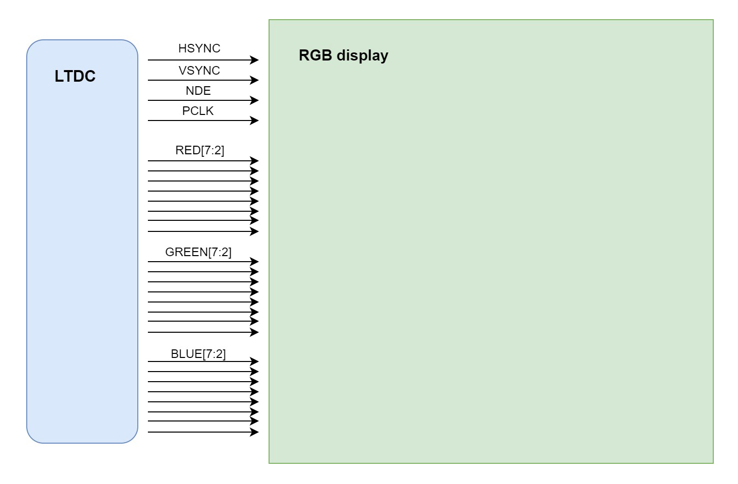
figure 5: LTDC signal lines. Only MSB are used if the display has less than 8 lines per color channel
Before enabling the LTDC we must configure the clock system. The LTDC uses a specific clock LCD_CLOCK to generate the pixel clock signal and it must be configured and enabled during the system initialization phase:
void system_clock_config(void)
{
  RCC_OscInitTypeDef RCC_OscInitStruct;
  RCC_ClkInitTypeDef RCC_ClkInitStruct;
  RCC_PeriphCLKInitTypeDef PeriphClkInitStruct;

  /* Configure the main internal regulator output voltage */
  __HAL_RCC_PWR_CLK_ENABLE();

  __HAL_PWR_VOLTAGESCALING_CONFIG(PWR_REGULATOR_VOLTAGE_SCALE1);

  /* Initialize the CPU, AHB and APB busses clocks */
  RCC_OscInitStruct.OscillatorType = RCC_OSCILLATORTYPE_HSI;
  RCC_OscInitStruct.HSIState = RCC_HSI_ON;
  RCC_OscInitStruct.HSICalibrationValue = 16;
  RCC_OscInitStruct.PLL.PLLState = RCC_PLL_ON;
  RCC_OscInitStruct.PLL.PLLSource = RCC_PLLSOURCE_HSI;
  RCC_OscInitStruct.PLL.PLLM = 8;
  RCC_OscInitStruct.PLL.PLLN = 180;
  RCC_OscInitStruct.PLL.PLLP = RCC_PLLP_DIV2;
  RCC_OscInitStruct.PLL.PLLQ = 7;
  HAL_RCC_OscConfig(&RCC_OscInitStruct);

  /* Activate the Over-Drive mode */
  HAL_PWREx_EnableOverDrive();

  /* Initialize the CPU, AHB and APB busses clocks */
  RCC_ClkInitStruct.ClockType = RCC_CLOCKTYPE_HCLK|RCC_CLOCKTYPE_SYSCLK|RCC_CLOCKTYPE_PCLK1|RCC_CLOCKTYPE_PCLK2;
  RCC_ClkInitStruct.SYSCLKSource = RCC_SYSCLKSOURCE_PLLCLK;
  RCC_ClkInitStruct.AHBCLKDivider = RCC_SYSCLK_DIV1;
  RCC_ClkInitStruct.APB1CLKDivider = RCC_HCLK_DIV4;
  RCC_ClkInitStruct.APB2CLKDivider = RCC_HCLK_DIV2;

  HAL_RCC_ClockConfig(&RCC_ClkInitStruct, FLASH_LATENCY_5);

  /* initialize LTDC LCD clock */
  PeriphClkInitStruct.PeriphClockSelection = RCC_PERIPHCLK_LTDC;
  PeriphClkInitStruct.PLLSAI.PLLSAIN = 60;
  PeriphClkInitStruct.PLLSAI.PLLSAIR = 5;
  PeriphClkInitStruct.PLLSAIDivR = RCC_PLLSAIDIVR_4;
  HAL_RCCEx_PeriphCLKConfig(&PeriphClkInitStruct);
}
The HAL_LTDC_MspInit() function, called at the beginning of LTDC_init() enables the LTDC peripheral clock and takes care of the low level hardware initialization:
void HAL_LTDC_MspInit(LTDC_HandleTypeDef *ltdc)
{
  GPIO_InitTypeDef GPIO_InitStructure;

  /* Enable the LTDC clock */
  __HAL_RCC_LTDC_CLK_ENABLE();

  /* Enable GPIOs clock */
  __HAL_RCC_GPIOA_CLK_ENABLE();
  __HAL_RCC_GPIOB_CLK_ENABLE();
  __HAL_RCC_GPIOC_CLK_ENABLE();
  __HAL_RCC_GPIOD_CLK_ENABLE();
  __HAL_RCC_GPIOF_CLK_ENABLE();
  __HAL_RCC_GPIOG_CLK_ENABLE();

	/* GPIOs Configuration */
	/*
	   +------------------------+-----------------------+----------------------------+
	   +                       LCD pins assignment                                   +
	   +------------------------+-----------------------+----------------------------+
	   |  LCD_TFT R2 <-> PC.10  |  LCD_TFT G2 <-> PA.06 |  LCD_TFT B2 <-> PD.06      |
	   |  LCD_TFT R3 <-> PB.00  |  LCD_TFT G3 <-> PG.10 |  LCD_TFT B3 <-> PG.11      |
	   |  LCD_TFT R4 <-> PA.11  |  LCD_TFT G4 <-> PB.10 |  LCD_TFT B4 <-> PG.12      |
	   |  LCD_TFT R5 <-> PA.12  |  LCD_TFT G5 <-> PB.11 |  LCD_TFT B5 <-> PA.03      |
	   |  LCD_TFT R6 <-> PB.01  |  LCD_TFT G6 <-> PC.07 |  LCD_TFT B6 <-> PB.08      |
	   |  LCD_TFT R7 <-> PG.06  |  LCD_TFT G7 <-> PD.03 |  LCD_TFT B7 <-> PB.09      |
	   -------------------------------------------------------------------------------
	            |  LCD_TFT HSYNC <-> PC.06  | LCDTFT VSYNC <->  PA.04 |
	            |  LCD_TFT CLK   <-> PG.07  | LCD_TFT DE   <->  PF.10 |
	             -----------------------------------------------------
	 */

  /* GPIOA configuration */
  GPIO_InitStructure.Pin = GPIO_PIN_3 | GPIO_PIN_4 | GPIO_PIN_6 | GPIO_PIN_11 | GPIO_PIN_12;
  GPIO_InitStructure.Mode = GPIO_MODE_AF_PP;
  GPIO_InitStructure.Pull = GPIO_NOPULL;
  GPIO_InitStructure.Speed = GPIO_SPEED_FAST;
  GPIO_InitStructure.Alternate= GPIO_AF14_LTDC;
  HAL_GPIO_Init(GPIOA, &GPIO_InitStructure);

  /* GPIOB configuration */
  GPIO_InitStructure.Pin = GPIO_PIN_8 | GPIO_PIN_9 | GPIO_PIN_10 | GPIO_PIN_11;
  HAL_GPIO_Init(GPIOB, &GPIO_InitStructure);

  /* GPIOC configuration */
  GPIO_InitStructure.Pin = GPIO_PIN_6 | GPIO_PIN_7 | GPIO_PIN_10;
  HAL_GPIO_Init(GPIOC, &GPIO_InitStructure);

  /* GPIOD configuration */
  GPIO_InitStructure.Pin = GPIO_PIN_3 | GPIO_PIN_6;
  HAL_GPIO_Init(GPIOD, &GPIO_InitStructure);

  /* GPIOF configuration */
  GPIO_InitStructure.Pin = GPIO_PIN_10;
  HAL_GPIO_Init(GPIOF, &GPIO_InitStructure);

  /* GPIOG configuration */
  GPIO_InitStructure.Pin = GPIO_PIN_6 | GPIO_PIN_7 | GPIO_PIN_11;
  HAL_GPIO_Init(GPIOG, &GPIO_InitStructure);

  /* GPIOB configuration */
  GPIO_InitStructure.Pin = GPIO_PIN_0 | GPIO_PIN_1;
  GPIO_InitStructure.Alternate= GPIO_AF9_LTDC;
  HAL_GPIO_Init(GPIOB, &GPIO_InitStructure);

  /* GPIOG configuration */
  GPIO_InitStructure.Pin = GPIO_PIN_10 | GPIO_PIN_12;
  HAL_GPIO_Init(GPIOG, &GPIO_InitStructure);
}
To display an image we must convert an image file to an array (possibly a const one, so it can be stored in flash memory) of bytes. To do this I used LCD image converter, a simple but powerful application that can convert a file to a variety of different pixel formats:
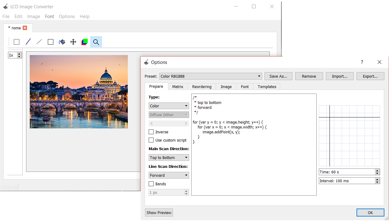
figure 6: LTDC image converter is used to generate a RGB888 image array
Once the image is converted to a byte array the generated header file is included and the array address can be used as the frame buffer starting address in the LTDC_LxCFBAR register. Layer window parameters are configured according to the image size (240 x 320, I rotated the image to fit the display in portrait mode).
figure 7: a 240 x 320 (rotated) image displayed
The second layer can be enabled as well and its contents drawn on top of layer 1. LTDC can manage transparency using the values in the LTDC_LxCACR Layer x Constant Alpha Configuration Register and LTDC_LxBFCR Layer x Blending Factor Configuration Register: here I used a constant alpha of 255 to obtain a 100% opacity (the value in the constant alpha register is divided by 255 by hardware so for example a value of 128 represents an alpha value of 0.5). Since the layer window is smaller than the display area the default layer background color is set to a transparent black (otherwise the default layer background color is used if the layer window is smaller than the display). The image is 110 x 110 pixels and the pixel format is ARGB8888 (the alpha channel is used to draw transparent pixels). Note that the LTDC_LxCBLR and LTDC_LxCBLNR registers are configured according to the image size: the LTDC always starts fetching data from the address defined in the LTDC_LxCFBAR register. I added the following lines of code to the LTDC_init() function to configure and enable layer 2:
/* configure layer 2 */
LTDC_Layer2->WHPCR = 139 + 20 << LTDC_LxWHPCR_WHSPPOS_Pos | 30 + 20 << LTDC_LxWHPCR_WHSTPOS_Pos;   // window horizontal start/stop positions
LTDC_Layer2->WVPCR = 113 + 200 << LTDC_LxWVPCR_WVSPPOS_Pos | 4 + 200 << LTDC_LxWVPCR_WVSTPOS_Pos;  // window vertical start/stop positions
LTDC_Layer2->PFCR = 0x00;                                                                          // ARGB8888 pixel format
LTDC_Layer2->DCCR = 0x00 << LTDC_LxDCCR_DCALPHA_Pos;                                               // layer default color (transparent black)
LTDC_Layer2->CFBAR = (uint32_t)stamp;                                                              // frame buffer start address
LTDC_Layer2->CFBLR = 110 * 4 << LTDC_LxCFBLR_CFBP_Pos | 110 * 4 + 3 << LTDC_LxCFBLR_CFBLL_Pos;     // frame buffer line length and pitch
LTDC_Layer2->CFBLNR = 110;                                                                         // frame buffer line number
LTDC_Layer2->CACR = 255;                                                                           // constant alpha
LTDC_Layer2->CR |= LTDC_LxCR_LEN;                                                                  // enable Layer2
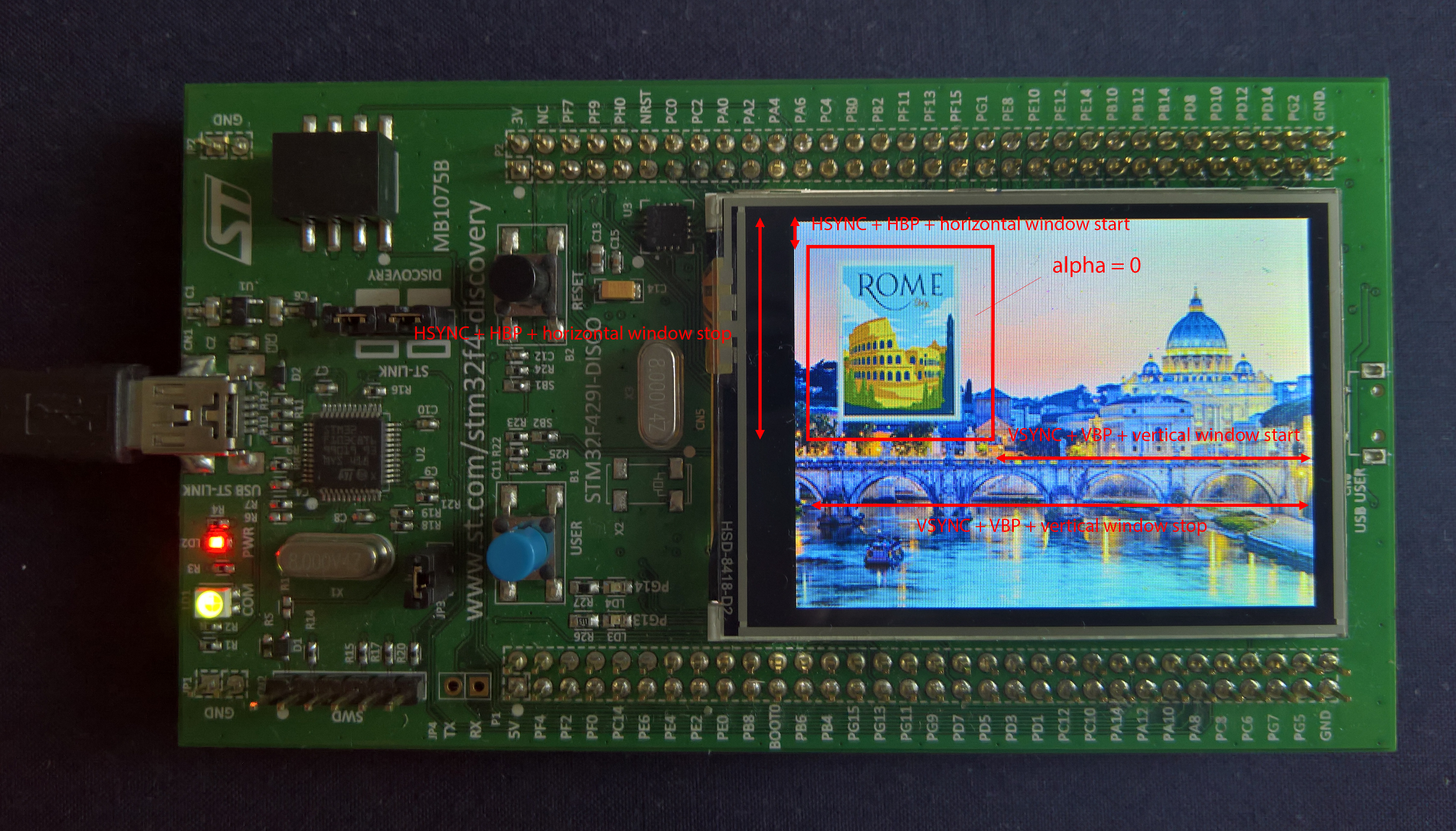
figure 8: the layer window must be inside the active display area. layer2 image is in ARGB8888 format, allowing tranparent pixels to show through
If we want do display portion of an image, we must configure LTDC_LxCBLR and LTDC_LxCBLNR accordingly:
/* configure layer 1 */
LTDC_Layer1->WHPCR = 129 + 50 << LTDC_LxWHPCR_WHSPPOS_Pos | 30 + 50 << LTDC_LxWHPCR_WHSTPOS_Pos;          // window horizontal start/stop positions
LTDC_Layer1->WVPCR = 103 + 50 << LTDC_LxWVPCR_WVSPPOS_Pos | 4 + 50 << LTDC_LxWVPCR_WVSTPOS_Pos;           // window vertical start/stop positions
LTDC_Layer1->PFCR = 0x01;   // RGB888 pixel format
LTDC_Layer1->DCCR = 0xFF << LTDC_LxDCCR_DCALPHA_Pos | 0xFF << LTDC_LxDCCR_DCGREEN_Pos;          // layer default color
LTDC_Layer1->CFBAR = (uint32_t)image;                                                           // frame buffer start address
LTDC_Layer1->CFBLR = 240 * 3 << LTDC_LxCFBLR_CFBP_Pos | 100 * 3 + 3 << LTDC_LxCFBLR_CFBLL_Pos;  // frame buffer line length and pitch
LTDC_Layer1->CFBLNR = 100;                                                                      // frame buffer line number
LTDC_Layer1->CACR = 255;                                                                        // constant alpha
Now I’m just showing 100 x 100 pixels of the layer 1 image so I configured the color buffer line length as 100 and the color buffer number of lines as 100. The line pitch value indicates that a framebuffer line is still 240 * 3 bytes long so the controller knows how to fetch bytes from the frame buffer correctly. I also moved the start of the window adding an offset of 50 pixels and 50 scan lines. The default background color is used where the layer isn’t used (the layer background color is a solid green):
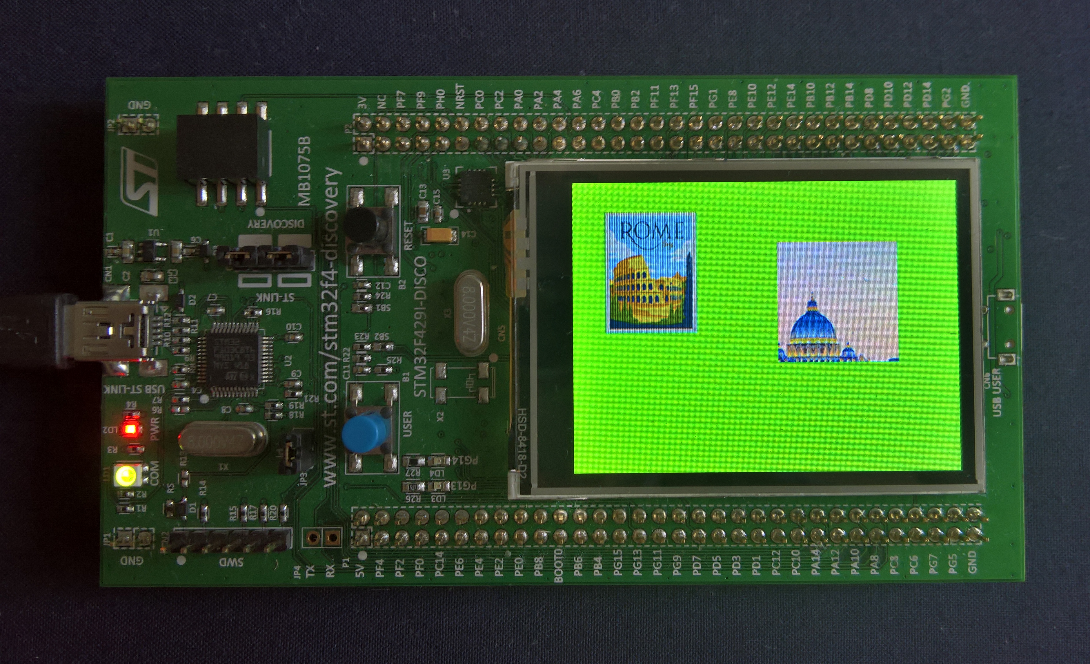
figure 9: layer1 window is resized and repositioned inside active display area
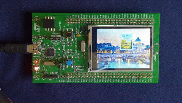
Using two layers and playing with the layer window size and position allows to create simple animations by simply moving the layer window around the frame:
#define SIZE                 110
#define DISPLAY_WIDTH        240
#define DISPLAY_HEIGHT       320
#define ACTIVE_AREA_START_X   30
#define ACTIVE_AREA_START_Y    4

int main(void)
{
  HAL_Init();
  system_clock_config();
  ILI9341_init();
  LTDC_init();

  double x_offset = 10;
  double y_offset = 10;
  double vx = 0.1;
  double vy = 0.1;

  for(;;)
  {
    if (x_offset <= 0 || x_offset + SIZE >= DISPLAY_WIDTH)
      vx = -vx;
    if (y_offset <= 0 || y_offset + SIZE >= DISPLAY_HEIGHT)
      vy = -vy;
    x_offset += vx;
    y_offset += vy;
    LTDC_Layer2->WHPCR = ACTIVE_AREA_START_X + SIZE + (int)x_offset - 1 << LTDC_LxWHPCR_WHSPPOS_Pos | ACTIVE_AREA_START_X + (int)x_offset << LTDC_LxWHPCR_WHSTPOS_Pos;
    LTDC_Layer2->WVPCR = ACTIVE_AREA_START_Y + SIZE + (int)y_offset - 1 << LTDC_LxWVPCR_WVSPPOS_Pos | ACTIVE_AREA_START_Y + (int)y_offset << LTDC_LxWVPCR_WVSTPOS_Pos;
    LTDC->SRCR = LTDC_SRCR_VBR;                      // reload shadow registers on vertical blanking period
    while ((LTDC->CDSR & LTDC_CDSR_VSYNCS) == 0)     // wait for next frame
	;
    while ((LTDC->CDSR & LTDC_CDSR_VSYNCS) == 1)
	;
  }
}
Shadow configuration registers are reloaded each vertical blanking period (after the last line has been drawn) and the code waits for the next frame by polling the VSYNCS flag of the LTDC_CDSR Current Display Status Register, whose bits contain the state of the synchronization signals (high if they’re asserted, no matter the polarity configured). Running the code we get a nice smooth animation:
LTDC interrupts
The LTDC controller has four interrupts logically OR-ed into two interrupt request lines:
- Register Reload Interrupt, generated as soon as the shadow registers are reloaded
- Line Interrupt, generated when a line number (programmed into LTDC_LIPCR Line Interrupt Position Control Register) is reached
- Transfer Error Interrupt, generated when an AHB bus error occurs during a transfer
- FIFO underrun Interrupt, generated when a pixel is requested from an empty layer FIFO
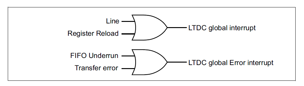
figure 10: LTDC interrupts and IRQ lines
The Line and Register Reload interrupts are useful to synchronize the code with the controller.
Using double buffering
Double buffer is used when we want the code to write on a frame buffer while another buffer is being read by the LTDC. This avoids corrupting the data being displayed on the screen. The buffers are switched during the vertical blanking period using polling or interrupts.
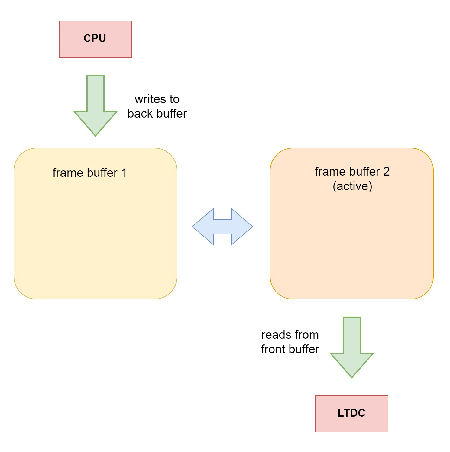
figure n: while the code writes to the back buffer the LTDC fetches data from the front (active) buffer. Famebuffers are switched during vertical blanking period.
In this example the framebuffers have a RGB888 color depth and for a 240×320 display that makes 225 KiB of memory for each buffer (3 bytes per pixel x 240 x 320 pixels) so they must be stored in external SRAM (the STM32F429I-DISCOVERY has a 64Mbit external SRAM so we’re good). The FMC Flexible Memory Controller has to be initialized and the address of the two frame buffers has to be configured. Drawing on the framebuffer is a matter of writing the right bytes in order to change the color. Once all pixels are drawn (bytes are written) the buffers are switched and the code can draw the next frame:
#define SDRAM_ADDR                               ((uint32_t)0xD0000000)                 // SDRAM bank 2 FMC address

/* double buffering (RGB888 frame buffer) */
#define FRAMEBUFFER_SIZE                         (DISPLAY_WIDTH * DISPLAY_HEIGHT * 3)
#define FRAMEBUFFER1_ADDR                        (SDRAM_ADDR)                           // frame buffer 1 address (external RAM)
#define FRAMEBUFFER2_ADDR                        (SDRAM_ADDR + FRAMEBUFFER_SIZE)        // frame buffer 2 address (external RAM)

enum framebuffer
{
  FRAMEBUFFER1,FRAMEBUFFER2
};

static enum framebuffer active = FRAMEBUFFER1;

void LTDC_init(void)
{
  /* initialize SDRAM */
  SDRAM_init();

  /* fill framebuffers with black */
  for (int i = 0 ; i < DISPLAY_WIDTH * DISPLAY_HEIGHT * 3 ; i++)
  	((int8_t*)FRAMEBUFFER1_ADDR)[i] = 0x00;
  for (int i = 0 ; i < DISPLAY_WIDTH * DISPLAY_HEIGHT * 3 ; i++)
	((int8_t*)FRAMEBUFFER2_ADDR)[i] = 0x00;

  /* LTDC initialization code */
  /* .................. */

  /* layer1 initialization code */
  /* .................. */
  LTDC_Layer1->CFBAR = FRAMEBUFFER1_ADDR;    // frame buffer 1 is the front buffer
  active = FRAMEBUFFER1;

  /* other LTDC initialization code */
  /* .................. */
}

void LTDC_switch_framebuffer(void)
{
  if (active == FRAMEBUFFER1)
  {
  	LTDC_Layer1->CFBAR = FRAMEBUFFER2_ADDR;
	active = FRAMEBUFFER2;
  }
  else
  {
	LTDC_Layer1->CFBAR = FRAMEBUFFER1_ADDR;
	active = FRAMEBUFFER1;
  }
  LTDC->SRCR = LTDC_SRCR_VBR;                     // reload shadow registers on vertical blank
  while ((LTDC->CDSR & LTDC_CDSR_VSYNCS) == 0)    // wait for reload
	;
}

uint8_t *LTDC_get_backbuffer_address(void)
{
  if (active == FRAMEBUFFER1)
	return (int8_t*)FRAMEBUFFER2_ADDR;
  else
	return (int8_t*)FRAMEBUFFER1_ADDR;
}
Now as soon as a frame is done with, calling LTDC_switch_framebuffer() waits for the vertical synchronization period and swaps the buffers. If the code is faster than the display refresh rate (70Hz in our case) it waits for the LTDC to complete drawing the frame.
In the next post I’m going to use the double buffer technique to draw and animate sprites.