
STM32F4: using the DMA controller
When we want to transfer data to/from a peripheral device to perform I/O operations we generally use memory mapped IO: peripherals’ configuration and control registers are mapped to the microcontroller memory space (for example in ARM Cortex-M processors devices are mapped to addresses 0x4000.0000 – 0x5FFF.FFFF) and the CPU moves data to/from peripherals writing to or reading from these addresses. This approach requires a lot of CPU overhead: it is the processor that moves data from peripheral to system memory and vice-versa. Some processors (like the STM32F429ZI on the STM32F429 Discovery board which I am using) have a dedicated DMA controller that can take control of the system bus, acting as a master, and allows for faster data transfers and less CPU overhead. DMA stands for Direct Memory Access and allows peripherals to initiate data transfers to or from memory without CPU intervention. In this article I will explain how to use the DMA in the STM32F429ZI to read in a number of samples from the Analog to Digital Converter.
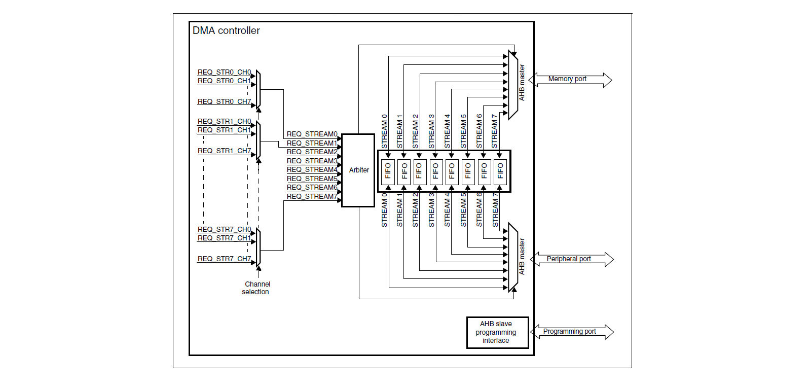
The DMA controller
The STM32F429ZI has two DMA controllers, each with 8 stream, and each stream has 8 channels (requests) each associated with a peripheral that can trigger a data transfer request when ready. Data tranfer direction can be from peripheral to memory, from memory to peripheral and from memory to memory (only DMA2 controller). The DMA controller has two AHB ports, one is the AHB memory port, to be connected to memories and one is the AHB peripheral port, to be connected to peripherals (the peripheral port of DMA2 is also connected to memories, in order to allow memory to memory transfers):
The AHB slave port is used to access the configuration registers and set up the DMA controller.
A DMA transaction consists of a number of data transfers of configurable width (byte, 16-bit halfword or 32-bit word). Each tranfer consists of three steps:
- a loading of data from peripheral data register or memory location addressed through DMA_SxPAR – DMA Stream x Peripheral Address Register or DMA_SxM0AR – DMA Stream x Memory Address Register 0 respectively.
- a storage of the loaded data into a memory location or a peripheral data register addressed through DMA_SxPAR or DMA_SxM0AR register respectively.
- a decrement of the value in DMA_SxNDTR – DMA Stream x Number of Data Register which contains the number of data tranfers still to be performed.
When a peripheral is ready it sends a request to the DMA controller asserting a signal. The DMA controller serves the request depending on the stream priority. As soon as the DMA access the peripheral it sends an acknowledge signal to the peripheral, which then deasserts its request. When the request is released the DMA deasserts the acknowledge signal.
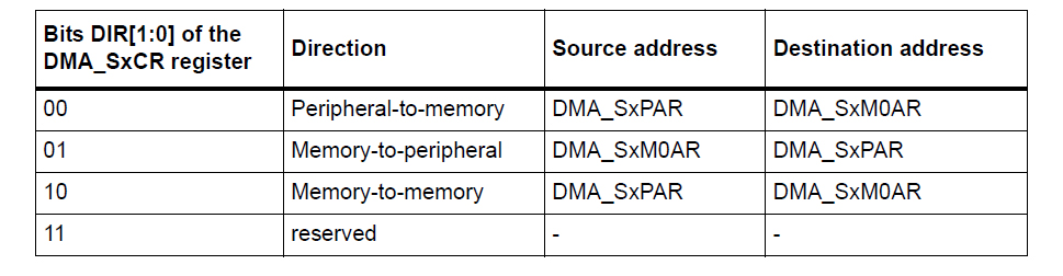
Configuring transfer direction and size
Data transfer direction can be configured by writing the DIR[1:0] bits in the DMA_SxCR – DMA Stream x Configuration Register:
The size of the trasfer can be configured by writing the PSIZE[1:0] (for the peripheral port) and MSIZE[1:0] (for the memory port) bits of DMA_SxCR register. Unless we’re using FIFO mode the width of the data for the source and destination must match (I explain FIFO mode later). If the size is a halfword or a word, the addresses of the source and destination (written in DMA_SxPAR and DMA_SxM0AR/DMA_SxM1AR registers) must be aligned to a 16-bit or 32-bit boundary respectively. The number of transfers in a DMA transaction is programmed into DMA_SxNDTR – DMA Stream x Number of Data Transfer Register: this register has 16 bits so the number of transfers goes from 0 to 65535. The value is decremented after each transfer.
Channel selection
Each stream is associated with a DMA request that can be selected out of 8 possible channel requests (peripherals). The selection is controlled by the CHSEL[2:0] bits in the DMA_SxCR register:
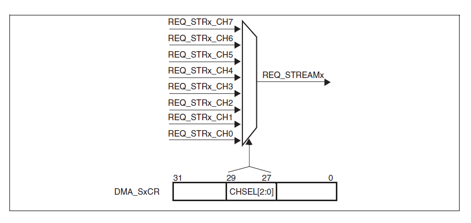
For example in the STM32F429ZI the ADC Analod to Digital Converter is on channel 0 of stream 0 of DMA2.
DMA modes
The DMA ca be used in direct mode or in FIFO mode: in direct mode FIFO buffering is disabled and every peripheral request triggers a single transfer to or from memory (in memory to peripheral transfers the FIFO is preloaded with the data to be transferred so data is ready as soon as a peripheral requests a transfer); when using direct mode the size of the source and destination must be the same and are both equal to PSIZE (MSIZE bits are ignored). FIFO mode is enabled by writing a 1 to DMDIS (Direct Mode Disable) bit in DMA_SxFCR – DMA Stream x FIFO Configuration Register . When using FIFO mode a four-word deep First In First Out buffer is used for each stream. The size of the source and destination data (PSIZE and MSIZE) can be different and the FIFO takes care of packing and unpacking data between source and destination. Burst tranfers are allowed in FIFO mode setting the MBURST[1:0] and PBURST[1:0] bits of DMA_SxCR. Each FIFO has a configurable threshold level that indicates when the FIFO must be filled again (when reading from the buffer) or flushed (when writing to the buffer). Using FIFO mode requires some complications so I’ll be using direct mode.
Peripheral and memory location addresses can be optionally incremented after each transfer or be fixed writing the PINC and MINC bits of DMA_SxCR register. Since I want to store a number of samples from the ADC into a buffer to compute a mean value I set the memory address to auto increment each transfer. The address pointer increments by a value equal to the data width configured in MSIZE (16 bits in this case).
Circular mode and double buffer mode
When the value in DMA_SxNDTR is zero all data transfers has been performed and the DMA transaction is complete. In Circular Mode after each transaction the DMA_SxNDTR register is reloaded with the initial value and another transaction begins. This feature can be enabled writing the CIRC bit in DMA_SxCR register. Circular mode is automatically enabled when using Double Buffer Mode. In double buffer mode the stream has two memory-side pointers, one is the location in the DMA_SxM0AR register and the second is the location in the DMA_SxM1AR register. When a transaction is done the two pointers are switched and another transaction begins, allowing the application to process the data in a buffer while the other is being filled or used by the DMA controller. Double buffering is enabled by setting the DBM bit in the DMA_SxCR register. I’ll use double buffering with circular mode so while the application is processing a batch of samples to compute a mean value the DMA will quietly continue to fill the other buffer with samples from ADC.
So this is the DMA initialization function so far:
static void DMA_init(void)
{
	/* enable DMA 2 clock */
	__HAL_RCC_DMA2_CLK_ENABLE();

	/* configure DMA2 */
	DMA2_Stream0->CR |= 0U << DMA_SxCR_ACK_Pos;       // ADC1 on DMA2 stream 0 channel 0
	DMA2_Stream0->CR |= 0x01 << DMA_SxCR_PSIZE_Pos;   // ADC data register is 16 bit (half word)
	DMA2_Stream0->CR |= 0x01 << DMA_SxCR_MSIZE_Pos;   // memory size is is 16 bit (half word)
	DMA2_Stream0->CR |= DMA_SxCR_DBM;                 // double buffer mode
	DMA2_Stream0->CR |= DMA_SxCR_MINC;                // memory increment (MSIZE = 16 bit)
	DMA2_Stream0->CR |= DMA_SxCR_CIRC;                // circular mode
	DMA2_Stream0->CR |= 0x00 << DMA_SxCR_DIR_Pos;     // peripheral to memory
	DMA2_Stream0->CR |= 0x03 << DMA_SxCR_PL_Pos;      // priority level very high
	DMA2_Stream0->PAR = (uint32_t)&ADC1->DR;          // peripheral base address
	DMA2_Stream0->M0AR = (uint32_t)sample_buffer0;    // memory base address 0
	DMA2_Stream0->M1AR = (uint32_t)sample_buffer1;    // memory base address 1
	DMA2_Stream0->NDTR = NUM_SAMPLES;                 // number of data
	DMA2_Stream0->FCR &= ~DMA_SxFCR_DMDIS;            // direct mode (FIFO disabled)
}
Synchronizing the application with the DMA: interrupts
For each DMA stream an interrupt can be generated. Five flags are OR-ed toghether and interrupts are triggered when an error occurs or when a transaction is half-finished or is done. Interrupts can be enabled by setting the corresponding enable bit in DMA_SxCR register. Every time a transaction is done a buffer is filled with values from the ADC so we can process the data. So I’ll enable a transaction complete interrupt by setting the TCIE Transfer Complete Interrupt Enable bit in the configuration register of stream 0:
static void DMA_init(void)
{
	/* rest of init code */
        ......
        ......

	/* enable DMA2 stream 0 interrupt */
	DMA2_Stream0->CR |= DMA_SxCR_TCIE;                // enable transfer complete interrupt
	NVIC_EnableIRQ(DMA2_Stream0_IRQn);                // enable stream 0 IRQ in NVIC

	/* enable DMA2 stream 0 */
	DMA2_Stream0->CR |= DMA_SxCR_EN;
}
Lastly, we enable the DMA controller by setting the EN Enable bit in the configuration register.
When a transaction is completed the transaction complete interrupt is triggered and the ISR processes the data in the current buffer:
void DMA2_Stream0_IRQHandler(void)
{
	/* transmission complete interrupt */
	if (DMA2->LISR & DMA_LISR_TCIF0 && DMA2_Stream0->CR & DMA_SxCR_TCIE)
	{
		DMA2->LIFCR = DMA_LIFCR_CTCIF0;  // acknowledge interrupt
		DMA_IRQHandler();
	}
}

void DMA_IRQHandler(void)
{
	uint16_t *p;
	if ((DMA2_Stream0->CR & DMA_SxCR_CT) == 0)  // current target buffer 0 (read buffer 1)
		p = sample_buffer1;
	else                                        // current target buffer 1 (read buffer 0)
		p = sample_buffer0;
	int acc_x = 0;
	int acc_y = 0;
	for (int i = 0 ; i < NUM_SAMPLES ; i += 2)
		acc_x += p[i];
	x_value = acc_x / NUM_SAMPLES;
	for (int i = 1 ; i < NUM_SAMPLES ; i += 2)
			acc_y += p[i];
	y_value = acc_y / NUM_SAMPLES;
}
The CT bit in DMA_SxCR indicates which of the two memory addresses programmed into DMA_SxM0AR and DMA_SxM1AR is currently being used by the DMA controller (sample_buffer1 and sample_buffer0 are arrays). The ISR acknowledge the interrupt and then checks which buffer is currently in use and process the data in the other buffer.
In this example I used the DMA and the ADC to sample data from two channels of an analog stick (x and y axis, so data are interleaved in the code) that I’m using as a joystick for a simple game that I describe in this post. It’s a simple Arkanoid clone but it sums up what I have shown about DMA and what I explain in this other post about driving a TFT display with the LTDC controller inside the STM32F4. Check it out for the complete source code.